VGA Signal Generation with the PIC32
Monday, May 22nd, 2017It all started after I had designed – and received from fabrication – a circuit board for prototyping cartridges for the Acorn Electron microcomputer. Although some prototyping had already taken place with an existing cartridge, with pins intended for ROM components being routed to drive other things, this board effectively “breaks out” all connections available to a cartridge that has been inserted into the computer’s Plus 1 expansion unit.
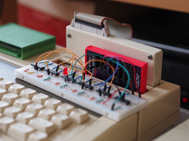
The Acorn Electron cartridge breakout board being used to drive an external circuit
One thing led to another, and soon my brother, David, was interfacing a microcontroller to the Electron in order to act as a peripheral being driven directly by the system’s bus signals. His approach involved having a program that would run and continuously scan the signals for read and write conditions and then interpret the address signals, sending and receiving data on the bus when appropriate.
Having acquired some PIC32 devices out of curiosity, with the idea of potentially interfacing them with the Electron, I finally took the trouble of looking at the datasheet to see whether some of the hard work done by David’s program might be handled by the peripheral hardware in the PIC32. The presence of something called “Parallel Master Port” was particularly interesting.
Operating this function in the somewhat insensitively-named “slave” mode, the device would be able to act like a memory device, with the signalling required by read and write operations mostly being dealt with by the hardware. Software running on the PIC32 would be able to read and write data through this port and be able to get notifications about new data while getting on with doing other things.
So began my journey into PIC32 experimentation, but this article isn’t about any of that, mostly because I put that particular investigation to one side after a degree of experience gave me perhaps a bit too much confidence, and I ended up being distracted by something far more glamorous: generating a video signal using the PIC32!
The Precedents’ Hall of Fame
There are plenty of people who have written up their experiments generating VGA and other video signals with microcontrollers. Here are some interesting examples:
- “VGA Video Generator” provides an introduction to VGA signal generation and gives circuit details as well as assembly language programs for AVR microcontrollers
- Craft is an impressive AVR-based “demo platform” producing video and audio
- “VGA On The Arduino With No External Parts Or CPU!” provides some good background detail on VGA signal generation and then describes how to get the secondary serial-to-USB microcontroller on certain Arduino devices to act as a video adapter
- “VGA output using a 36-pin STM32” provides some helpful signal details and implementation suggestions
And there are presumably many more pages on the Web with details of people sending pixel data over a cable to a display of some sort, often trying to squeeze every last cycle out of their microcontroller’s instruction processing unit. But, given an awareness of how microcontrollers should be able to take the burden off the programs running on them, employing peripheral hardware to do the grunt work of switching pins on and off at certain frequencies, maybe it would be useful to find examples of projects where such advantages of microcontrollers had been brought to bear on the problem.
In fact, I was already aware of the Maximite “single chip computer” partly through having seen the cloned version of the original being sold by Olimex – something rather resented by the developer of the Maximite for reasons largely rooted in an unfortunate misunderstanding of Free Software licensing on his part – and I was aware that this computer could generate a VGA signal. Indeed, the method used to achieve this had apparently been written up in a textbook for the PIC32 platform, albeit generating a composite video signal using one of the on-chip SPI peripherals. The Colour Maximite uses three SPI channels to generate one red, one green, and one blue channel of colour information, thus supporting eight-colour graphical output.
But I had been made aware of the Parallel Master Port (PMP) and its “master” mode, used to drive LCD panels with eight bits of colour information per pixel (or, using devices with many more pins than those I had acquired, with sixteen bits of colour information per pixel). Would it surely not be possible to generate 256-colour graphical output at the very least?
Information from people trying to use PMP for this purpose was thin on the ground. Indeed, reading again one article that mentioned an abandoned attempt to get PMP working in this way, using the peripheral to emit pixel data for display on a screen instead of a panel, I now see that it actually mentions an essential component of the solution that I finally arrived at. But the author had unfortunately moved away from that successful component in an attempt to get the data to the display at a rate regarded as satisfactory.
Direct Savings
It is one thing to have the means to output data to be sent over a cable to a display. It is another to actually send the data efficiently from the microcontroller. Having contemplated such issues in the past, it was not a surprise that the Maximite and other video-generating solutions use direct memory access (DMA) to get the hardware, as opposed to programs, to read through memory and to write its contents to a destination, which in most cases seemed to be the memory address holding output data to be emitted via a data pin using the SPI mechanism.
I had also envisaged using DMA and was still fixated on using PMP to emit the different data bits to the output circuit producing the analogue signals for the display. Indeed, Microchip promotes the PMP and DMA combination as a way of doing “low-cost controllerless graphics solutions” involving LCD panels, so I felt that there surely couldn’t be much difference between that and getting an image on my monitor via a few resistors on the breadboard.
And so, a tour of different PIC32 features began, trying to understand the DMA documentation, the PMP documentation, all the while trying to get a grasp of what the VGA signal actually looks like, the timing constraints of the various synchronisation pulses, and battle various aspects of the MIPS architecture and the PIC32 implementation of it, constantly refining my own perceptions and understanding and learning perhaps too often that there may have been things I didn’t know quite enough about before trying them out!
Using VGA to Build a Picture
Before we really start to look at a VGA signal, let us first look at how a picture is generated by the signal on a screen:
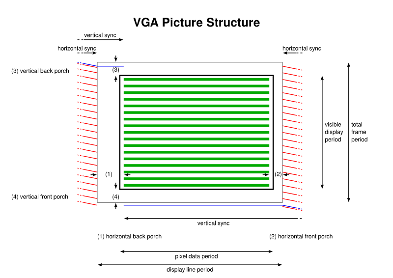
The structure of a display image or picture produced by a VGA signal
The most important detail at this point is the central area of the diagram, filled with horizontal lines representing the colour information that builds up a picture on the display, with the actual limits of the screen being represented here by the bold rectangle outline. But it is also important to recognise that even though there are a number of visible “display lines” within which the colour information appears, the entire “frame” sent to the display actually contains yet more lines, even though they will not be used to produce an image.
Above and below – really before and after – the visible display lines are the vertical back and front porches whose lines are blank because they do not appear on the screen or are used to provide a border at the top and bottom of the screen. Such extra lines contribute to the total frame period and to the total number of lines dividing up the total frame period.
Figuring out how many lines a display will have seems to involve messing around with something called the “generalised timing formula”, and if you have an X server like Xorg installed on your system, you may even have a tool called “gtf” that will attempt to calculate numbers of lines and pixels based on desired screen resolutions and frame rates. Alternatively, you can look up some common sets of figures on sites providing such information.
What a VGA Signal Looks Like
Some sources show diagrams attempting to describe the VGA signal, but many of these diagrams are open to interpretation (in some cases, very much so). They perhaps show the signal for horizontal (display) lines, then other signals for the entire image, but they either do not attempt to combine them, or they instead combine these details ambiguously.
For instance, should the horizontal sync (synchronisation) pulse be produced when the vertical sync pulse is active or during the “blanking” period when no pixel information is being transmitted? This could be deduced from some diagrams but only if you share their authors’ unstated assumptions and do not consider other assertions about the signal structure. Other diagrams do explicitly show the horizontal sync active during vertical sync pulses, but this contradicts statements elsewhere such as “during the vertical sync period the horizontal sync must also be held low”, for instance.
After a lot of experimentation, I found that the following signal structure was compatible with the monitor I use with my computer:
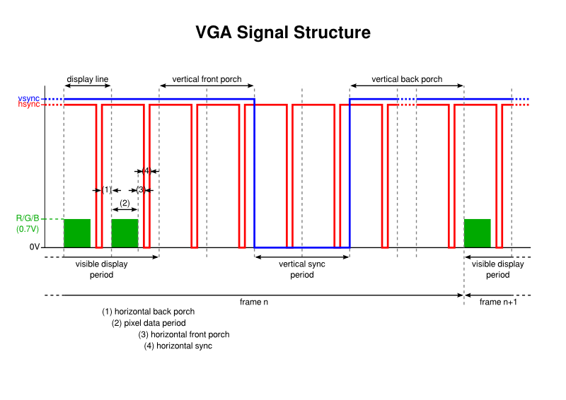
The basic structure of a VGA signal, or at least a signal that my monitor can recognise
There are three principal components to the signal:
- Colour information for the pixel or line data forms the image on the display and it is transferred within display lines during what I call the visible display period in every frame
- The horizontal sync pulse tells the display when each horizontal display line ends, or at least the frequency of the lines being sent
- The vertical sync pulse tells the display when each frame (or picture) ends, or at least the refresh rate of the picture
The voltage levels appear to be as follows:
- Colour information should be at 0.7V (although some people seem to think that 1V is acceptable as “the specified peak voltage for a VGA signal”)
- Sync pulses are supposed to be at “TTL” levels, which apparently can be from 0V to 0.5V for the low state and from 2.7V to 5V for the high state
Meanwhile, the polarity of the sync pulses is also worth noting. In the above diagram, they have negative polarity, meaning that an active pulse is at the low logic level. Some people claim that “modern VGA monitors don’t care about sync polarity”, but since it isn’t clear to me what determines the polarity, and since most descriptions and demonstrations of VGA signal generation seem to use negative polarity, I chose to go with the flow. As far as I can tell, the gtf tool always outputs the same polarity details, whereas certain resources provide signal characteristics with differing polarities.
It is possible, and arguably advisable, to start out trying to generate sync pulses and just grounding the colour outputs until your monitor (or other VGA-capable display) can be persuaded that it is receiving a picture at a certain refresh rate and resolution. Such confirmation can be obtained on a modern display by seeing a blank picture without any “no signal” or “input not supported” messages and by being able to activate the on-screen menu built into the device, in which an option is likely to exist to show the picture details.
How the sync and colour signals are actually produced will be explained later on. This section was merely intended to provide some background and gather some fairly useful details into one place.
Counting Lines and Generating Vertical Sync Pulses
The horizontal and vertical sync pulses are each driven at their own frequency. However, given that there are a fixed number of lines in every frame, it becomes apparent that the frequency of vertical sync pulse occurrences is related to the frequency of horizontal sync pulses, the latter occurring once per line, of course.
With, say, 622 lines forming a frame, the vertical sync will occur once for every 622 horizontal sync pulses, or at a rate that is 1/622 of the horizontal sync frequency or “line rate”. So, if we can find a way of generating the line rate, we can not only generate horizontal sync pulses, but we can also count cycles at this frequency, and every 622 cycles we can produce a vertical sync pulse.
But how do we calculate the line rate in the first place? First, we decide what our refresh rate should be. The “classic” rate for VGA output is 60Hz. Then, we decide how many lines there are in the display including those extra non-visible lines. We multiply the refresh rate by the number of lines to get the line rate:
60Hz * 622 = 37320Hz = 37.320kHz
On a microcontroller, the obvious way to obtain periodic events is to use a timer. Given a particular frequency at which the timer is updated, a quick calculation can be performed to discover how many times a timer needs to be incremented before we need to generate an event. So, let us say that we have a clock frequency of 24MHz, and a line rate of 37.320kHz, we calculate the number of timer increments required to produce the latter from the former:
24MHz / 37.320kHz = 24000000Hz / 37320Hz = 643
So, if we set up a timer that counts up to 642 and then upon incrementing again to 643 actually starts again at zero, with the timer sending a signal when this “wraparound” occurs, we can have a mechanism providing a suitable frequency and then make things happen at that frequency. And this includes counting cycles at this particular frequency, meaning that we can increment our own counter by 1 to keep track of display lines. Every 622 display lines, we can initiate a vertical sync pulse.
One aspect of vertical sync pulses that has not yet been mentioned is their duration. Various sources suggest that they should last for only two display lines, although the “gtf” tool specifies three lines instead. Our line-counting logic therefore needs to know that it should enable the vertical sync pulse by bringing it low at a particular starting line and then disable it by bringing it high again after two whole lines.
Generating Horizontal Sync Pulses
Horizontal sync pulses take place within each display line, have a specific duration, and they must start at the same time relative to the start of each line. Some video output demonstrations seem to use lots of precisely-timed instructions to achieve such things, but we want to use the peripherals of the microcontroller as much as possible to avoid wasting CPU time. Having considered various tricks involving specially formulated data that might be transferred from memory to act as a pulse, I was looking for examples of DMA usage when I found a mention of something called the Output Compare unit on the PIC32.
What the Output Compare (OC) units do is to take a timer as input and produce an output signal dependent on the current value of the timer relative to certain parameters. In clearer terms, you can indicate a timer value at which the OC unit will cause the output to go high, and you can indicate another timer value at which the OC unit will cause the output to go low. It doesn’t take much imagination to realise that this sounds almost perfect for generating the horizontal sync pulse:
- We take the timer previously set up which counts up to 643 and thus divides the display line period into units of 1/643.
- We identify where the pulse should be brought low and present that as the parameter for taking the output low.
- We identify where the pulse should be brought high and present that as the parameter for taking the output high.
Upon combining the timer and the OC unit, then configuring the output pin appropriately, we end up with a low pulse occurring at the line rate, but at a suitable offset from the start of each line.
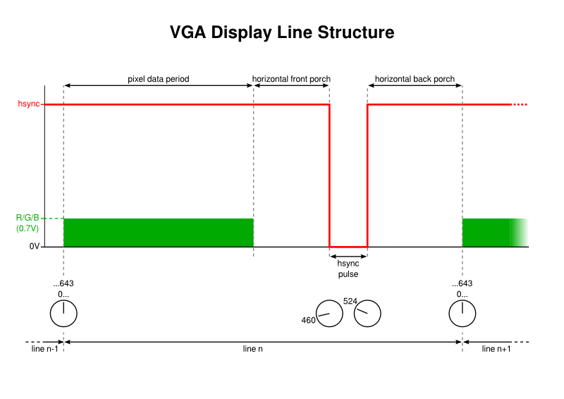
The structure of each visible display line in the VGA signal
In fact, the OC unit also proves useful in actually generating the vertical sync pulses, too. Although we have a timer that can tell us when it has wrapped around, we really need a mechanism to act upon this signal promptly, at least if we are to generate a clean signal. Unfortunately, handling an interrupt will introduce a delay between the timer wrapping around and the CPU being able to do something about it, and it is not inconceivable that this delay may vary depending on what the CPU has been doing.
So, what seems to be a reasonable solution to this problem is to count the lines and upon seeing that the vertical sync pulse should be initiated at the start of the next line, we can enable another OC unit configured to act as soon as the timer value is zero. Thus, upon wraparound, the OC unit will spring into action and bring the vertical sync output low immediately. Similarly, upon realising that the next line will see the sync pulse brought high again, we can reconfigure the OC unit to do so as soon as the timer value again wraps around to zero.
Inserting the Colour Information
At this point, we can test the basic structure of the signal and see if our monitor likes it. But none of this is very interesting without being able to generate a picture, and so we need a way of getting pixel information from the microcontroller’s memory to its outputs. We previously concluded that Direct Memory Access (DMA) was the way to go in reading the pixel data from what is usually known as a framebuffer, sending it to another place for output.
As previously noted, I thought that the Parallel Master Port (PMP) might be the right peripheral to use. It provides an output register, confusingly called the PMDIN (parallel master data in) register, that lives at a particular address and whose value is exposed on output pins. On the PIC32MX270, only the least significant eight bits of this register are employed in emitting data to the outside world, and so a DMA destination having a one-byte size, located at the address of PMDIN, is chosen.
The source data is the framebuffer, of course. For various retrocomputing reasons hinted at above, I had decided to generate a picture 160 pixels in width, 256 lines in height, and with each byte providing eight bits of colour depth (specifying how many distinct colours are encoded for each pixel). This requires 40 kilobytes and can therefore reside in the 64 kilobytes of RAM provided by the PIC32MX270. It was at this point that I learned a few things about the DMA mechanisms of the PIC32 that didn’t seem completely clear from the documentation.
Now, the documentation talks of “transactions”, “cells” and “blocks”, but I don’t think it describes them as clearly as it could do. Each “transaction” is just a transfer of a four-byte word. Each “cell transfer” is a collection of transactions that the DMA mechanism performs in a kind of batch, proceeding with these as quickly as it can until it either finishes the batch or is told to stop the transfer. Each “block transfer” is a collection of cell transfers. But what really matters is that if you want to transfer a certain amount of data and not have to keep telling the DMA mechanism to keep going, you need to choose a cell size that defines this amount. (When describing this, it is hard not to use the term “block” rather than “cell”, and I do wonder why they assigned these terms in this way because it seems counter-intuitive.)
You can perhaps use the following template to phrase your intentions:
I want to transfer <cell size> bytes at a time from a total of <block size> bytes, reading data starting from <source address>, having <source size>, and writing data starting at <destination address>, having <destination size>.
The total number of bytes to be transferred – the block size – is calculated from the source and destination sizes, with the larger chosen to be the block size. If we choose a destination size less than the source size, the transfers will not go beyond the area of memory defined by the specified destination address and the destination size. What actually happens to the “destination pointer” is not immediately obvious from the documentation, but for our purposes, where we will use a destination size of one byte, the DMA mechanism will just keep writing source bytes to the same destination address over and over again. (One might imagine the pointer starting again at the initial start address, or perhaps stopping at the end address instead.)
So, for our purposes, we define a “cell” as 160 bytes, being the amount of data in a single display line, and we only transfer one cell in a block. Thus, the DMA source is 160 bytes long, and even though the destination size is only a single byte, the DMA mechanism will transfer each of the source bytes into the destination. There is a rather unhelpful diagram in the documentation that perhaps tries to communicate too much at once, leading one to believe that the cell size is a factor in how the destination gets populated by source data, but the purpose of the cell size seems only to be to define how much data is transferred at once when a transfer is requested.
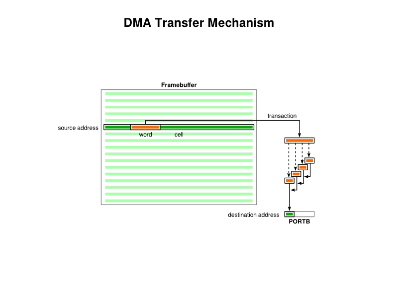
The transfer of framebuffer data to PORTB using DMA cell transfers (noting that this hints at the eventual approach which uses PORTB and not PMDIN)
In the matter of requesting a transfer, we have already described the mechanism that will allow us to make this happen: when the timer signals the start of a new line, we can use the wraparound event to initiate a DMA transfer. It would appear that the transfer will happen as fast as both the source and the destination will allow, at least as far as I can tell, and so it is probably unlikely that the data will be sent to the destination too quickly. Once the transfer of a line’s pixel data is complete, we can do some things to set up the transfer for the next line, like changing the source data address to point to the next 160 bytes representing the next display line.
(We could actually set the block size to the length of the entire framebuffer – by setting the source size – and have the DMA mechanism automatically transfer each line in turn, updating its own address for the current line. However, I intend to support hardware scrolling, where the address of the first line of the screen can be adjusted so that the display starts part way through the framebuffer, reaches the end of the framebuffer part way down the screen, and then starts again at the beginning of the framebuffer in order to finish displaying the data at the bottom of the screen. The DMA mechanism doesn’t seem to support the necessary address wraparound required to manage this all by itself.)
Output Complications
Having assumed that the PMP peripheral would be an appropriate choice, I soon discovered some problems with the generated output. Although the data that I had stored in the RAM seemed to be emitted as pixels in appropriate colours, there were gaps between the pixels on the screen. Yet the documentation seemed to vaguely indicate that the PMDIN register was more or less continuously updated. That meant that the actual output signals were being driven low between each pixel, causing black-level gaps and ruining the result.
I wondered if anything could be done about this issue. PMP is really intended as some kind of memory interface, and it isn’t unreasonable for it to only maintain valid data for certain periods of time, modifying control signals to define this valid data period. That PMP can be used to drive LCD panels is merely a result of those panels themselves upholding this kind of interface. For those of you familiar with microcontrollers, the solution to my problem was probably obvious several paragraphs ago, but it needed me to reconsider my assumptions and requirements before I realised what I should have been doing all along.
Unlike SPI, which concerns itself with the bit-by-bit serial output of data, PMP concerns itself with the multiple-bits-at-once parallel output of data, and all I wanted to do was to present multiple bits to a memory location and have them translated to a collection of separate signals. But, of course, this is exactly how normal I/O (input/output) pins are provided on microcontrollers! They all seem to provide “PORT” registers whose bits correspond to output pins, and if you write a value to those registers, all the pins can be changed simultaneously. (This feature is obscured by platforms like Arduino where functions are offered to manipulate only a single pin at once.)
And so, I changed the DMA destination to be the PORTB register, which on the PIC32MX270 is the only PORT register with enough bits corresponding to I/O pins to be useful enough for this application. Even then, PORTB does not have a complete mapping from bits to pins: some pins that are available in other devices have been dedicated to specific functions on the PIC32MX270F256B and cannot be used for I/O. So, it turns out that we can only employ at most seven bits of our pixel data in generating signal data:
| Pins | ||||||||||||||||
|---|---|---|---|---|---|---|---|---|---|---|---|---|---|---|---|---|
| … | 15 | 14 | 13 | 12 | 11 | 10 | 9 | 8 | 7 | 6 | 5 | 4 | 3 | 2 | 1 | 0 |
| … | RPB15 | RPB14 | RPB13 | RPB11 | RPB10 | RPB9 | RPB8 | RPB7 | RPB5 | RPB4 | RPB3 | RPB2 | RPB1 | RPB0 | ||
We could target the first byte of PORTB (bits 0 to 7) or the second byte (bits 8 to 15), but either way we will encounter an unmapped bit. So, instead of choosing a colour representation making use of eight bits, we have to make do with only seven.
Initially, not noticing that RPB6 was not available, I was using a “RRRGGGBB” or “332” representation. But persuaded by others in a similar predicament, I decided to choose a representation where each colour channel gets two bits, and then a separate intensity bit is used to adjust the final intensity of the basic colour result. This also means that greyscale output is possible because it is possible to balance the channels.
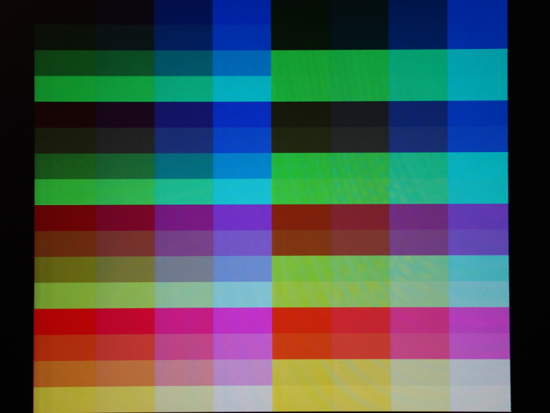
The colours employing two bits per channel plus one intensity bit, perhaps not shown completely accurately due to circuit inadequacies and the usual white balance issues when taking photographs
It is worth noting at this point that since we have left the 8-bit limitations of the PMP peripheral far behind us now, we could choose to populate two bytes of PORTB at once, aiming for sixteen bits per pixel but actually getting fourteen bits per pixel once the unmapped bits have been taken into account. However, this would double our framebuffer memory requirements for the same resolution, and we don’t have that much memory. There may be devices with more than sixteen bits mapped in the 32-bit PORTB register (or in one of the other PORT registers), but they had better have more memory to be useful for greater colour depths.
Back in Black
One other matter presented itself as a problem. It is all very well generating a colour signal for the pixels in the framebuffer, but what happens at the end of each DMA transfer once a line of pixels has been transmitted? For the portions of the display not providing any colour information, the channel signals should be held at zero, yet it is likely that the last pixel on any given line is not at the lowest possible (black) level. And so the DMA transfer will have left a stray value in PORTB that could then confuse the monitor, producing streaks of colour in the border areas of the display, making the monitor unsure about the black level in the signal, and also potentially confusing some monitors about the validity of the picture, too.
As with the horizontal sync pulses, we need a prompt way of switching off colour information as soon as the pixel data has been transferred. We cannot really use an Output Compare unit because that only affects the value of a single output pin, and although we could wire up some kind of blanking in our external circuit, it is simpler to look for a quick solution within the capabilities of the microcontroller. Fortunately, such a quick solution exists: we can “chain” another DMA channel to the one providing the pixel data, thereby having this new channel perform a transfer as soon as the pixel data has been sent in its entirety. This new channel has one simple purpose: to transfer a single byte of black pixel data. By doing this, the monitor will see black in any borders and beyond the visible regions of the display.
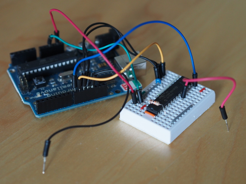
Wiring Up
Of course, the microcontroller still has to be connected to the monitor somehow. First of all, we need a way of accessing the pins of a VGA socket or cable. One reasonable approach is to obtain something that acts as a socket and that breaks out the different signals from a cable, connecting the microcontroller to these broken-out signals.
Wanting to get something for this task quickly and relatively conveniently, I found a product at a local retailer that provides a “male” VGA connector and screw-adjustable terminals to break out the different pins. But since the VGA cable also has a male connector, I also needed to get a “gender changer” for VGA that acts as a “female” connector in both directions, thus accommodating the VGA cable and the male breakout board connector.
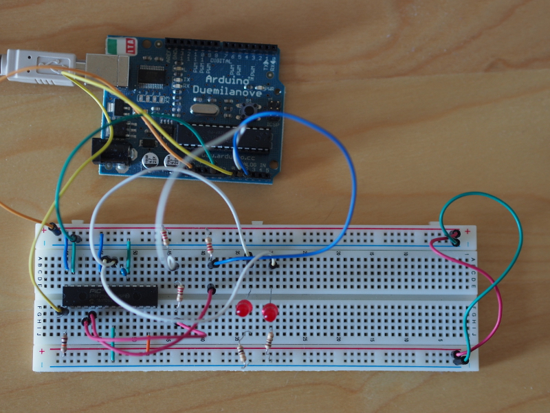
Wiring up to the broken-out VGA connector pins is mostly a matter of following diagrams and the pin numbering scheme, illustrated well enough in various resources (albeit with colour signal transposition errors in some resources). Pins 1, 2 and 3 need some special consideration for the red, green and blue signals, and we will look at them in a moment. However, pins 13 and 14 are the horizontal and vertical sync pins, respectively, and these can be connected directly to the PIC32 output pins in this case, since the 3.3V output from the microcontroller is supposedly compatible with the “TTL” levels. Pins 5 through 10 can be connected to ground.
We have seen mentions of colour signals with magnitudes of up to 0.7V, but no explicit mention of how they are formed has been presented in this article. Fortunately, everyone is willing to show how they converted their digital signals to an analogue output, with most of them electing to use a resistor network to combine each output pin within a channel to produce a hopefully suitable output voltage.
Here, with two bits per channel, I take the most significant bit for a channel and send it through a 470ohm resistor. Meanwhile, the least significant bit for the channel is sent through a 1000ohm resistor. Thus, the former contributes more to the magnitude of the signal than the latter. If we were only dealing with channel information, this would be as much as we need to do, but here we also employ an intensity bit whose job it is to boost the channels by a small amount, making sure not to allow the channels to pollute each other via this intensity sub-circuit. Here, I feed the intensity output through a 2200ohm resistor and then to each of the channel outputs via signal diodes.
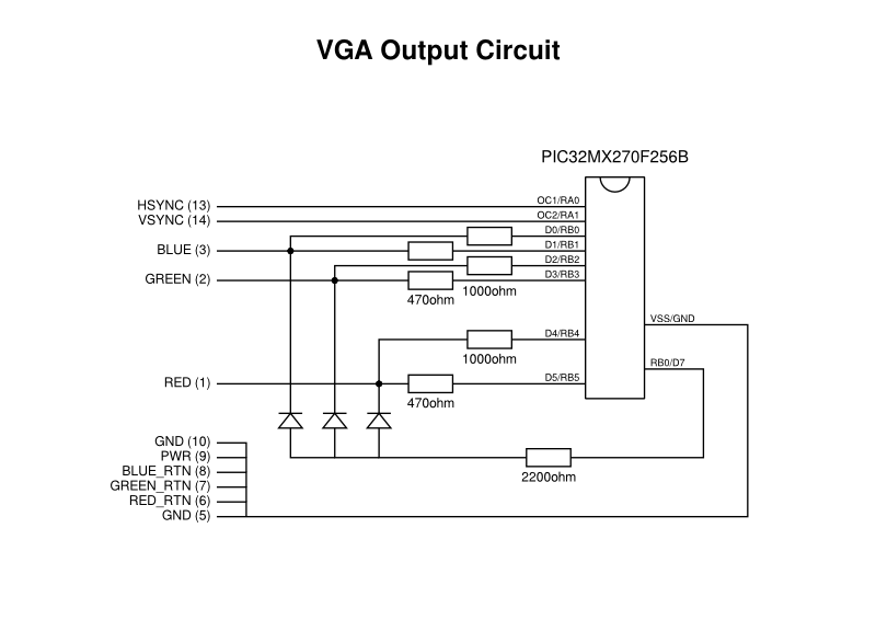
The circuit showing connections relevant to VGA output (generic connections are not shown)
The Final Picture
I could probably go on and cover other aspects of the solution, but the fundamental aspects are probably dealt with sufficiently above to help others reproduce this experiment themselves. Populating memory with usable image data, at least in this solution, involves copying data to RAM, and I did experience problems with accessing RAM that are probably related to CPU initialisation (as covered in my previous article) and to synchronising the memory contents with what the CPU has written via its cache.
As for the actual picture data, the RGB-plus-intensity representation is not likely to be the format of most images these days. So, to prepare data for output, some image processing is needed. A while ago, I made a program to perform palette optimisation and dithering on images for the Acorn Electron, and I felt that it was going to be easier to adapt the dithering code than it was to figure out the necessary techniques required for software like ImageMagick or the Python Imaging Library. The pixel data is then converted to assembly language data definition statements and incorporated into my PIC32 program.
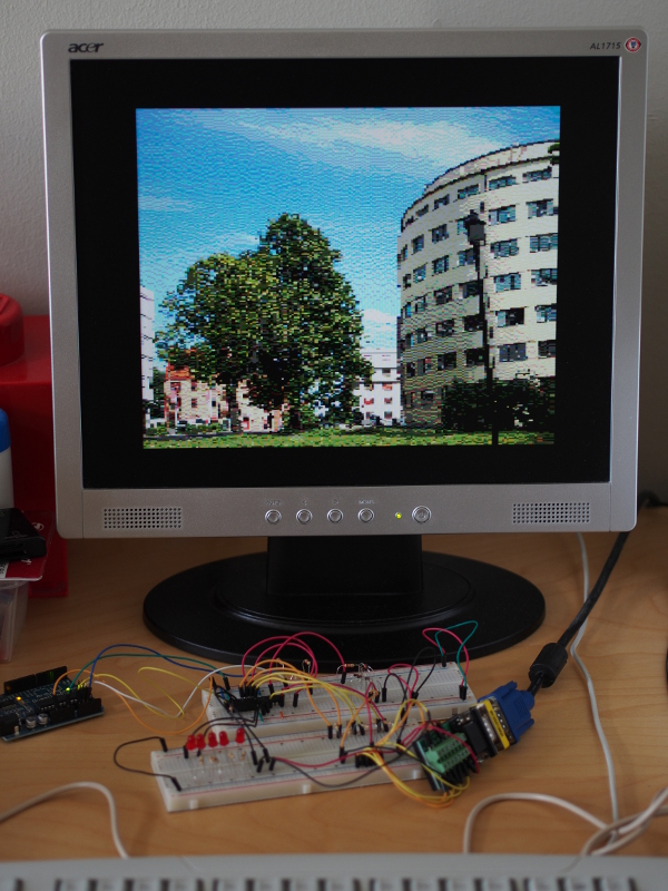
VGA output from a PIC32 microcontroller, featuring a picture showing some Oslo architecture, with the PIC32MX270 being powered (and programmed) by the Arduino Duemilanove, and with the breadboards holding the necessary resistors and diodes to supply the VGA breakout and, beyond that, the cable to the monitor
To demonstrate control over the visible region, I deliberately adjusted the display frequencies so that the monitor would consider the signal to be carrying an image 800 pixels by 600 pixels at a refresh rate of 60Hz. Since my framebuffer is only 256 lines high, I double the lines to produce 512 lines for the display. It would seem that choosing a line rate to try and produce 512 lines has the monitor trying to show something compatible with the traditional 640×480 resolution and thus lines are lost off the screen. I suppose I could settle for 480 lines or aim for 300 lines instead, but I actually don’t mind having a border around the picture.
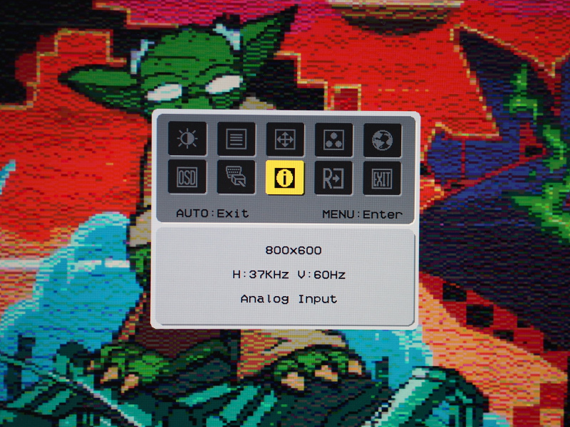
The on-screen menu showing the monitor's interpretation of the signal
It is worth noting that I haven’t really mentioned a “pixel clock” or “dot clock” so far. As far as the display receiving the VGA signal is concerned, there is no pixel clock in that signal. And as far as we are concerned, the pixel clock is only important when deciding how quickly we can get our data into the signal, not in actually generating the signal. We can generate new colour values as slowly (or as quickly) as we might like, and the result will be wider (or narrower) pixels, but it shouldn’t make the actual signal invalid in any way.
Of course, it is important to consider how quickly we can generate pixels. Previously, I mentioned a 24MHz clock being used within the PIC32, and it is this clock that is used to drive peripherals and this clock’s frequency that will limit the transfer speed. As noted elsewhere, a pixel clock frequency of 25MHz is used to support the traditional VGA resolution of 640×480 at 60Hz. With the possibilities of running the “peripheral clock” in the PIC32MX270 considerably faster than this, it becomes a matter of experimentation as to how many pixels can be supported horizontally.
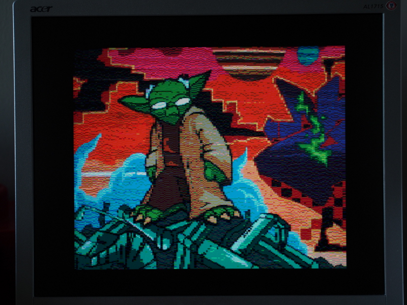
Some Oslo street art being displayed by the PIC32
For my own purposes, I have at least reached the initial goal of generating a stable and usable video signal. Further work is likely to involve attempting to write routines to modify the framebuffer, maybe support things like scrolling and sprites, and even consider interfacing with other devices.
Naturally, this project is available as Free Software from its own repository. Maybe it will inspire or encourage you to pursue something similar, knowing that you absolutely do not need to be any kind of “expert” to stubbornly persist and to eventually get results!