Paul Boddie's Free Software-related blog
Paul's activities and perspectives around Free Software
Hardware Experiments with Fritzing
One of my other interests, if you can even regard it as truly separate to my interests in Free Software and open hardware, involves the microcomputer systems of the 1980s that first introduced me to computing and probably launched me in the direction of my current career. There are many aspects of such systems that invite re-evaluation of their capabilities and limitations, leading to the consideration of improvements that could have been made at the time, as well as more radical enhancements that unashamedly employ technology that has only become available or affordable in recent years. Such “what if?” thought experiments and their hypothetical consequences are useful if we are to learn from the strategic mistakes once made by systems vendors, to have an informed perspective on current initiatives, and to properly appreciate computing history.
At the same time, people still enjoy actually using such systems today, writing new software and providing hardware that makes such continuing usage practical and sustainable. These computers and their peripherals are certainly “getting on”, and acquiring or rediscovering such old systems does not necessarily mean that you can plug them in and they still work as if they were new. Indeed, the lifetime of magnetic media and the devices that can read it, together with issues of physical decay in some components, mean that alternative mechanisms for loading and storing software have become attractive for some users, having been developed to complement or replace the cassette tape and floppy disk methods that those of us old enough to remember would have used “back in the day”.
My microcomputer of choice in the 1980s was the Acorn Electron – a cut-down, less expensive version of the BBC Microcomputer hardware platform – which supported only cassette storage in its unexpanded form. However, some expansion units added the disk interfaces present on the BBC Micro, while others added the ability to use ROM-based software. On the BBC Micro, one would plug ROM chips directly into sockets, and some expansion units for the Electron supported this method, too. The official Plus 1 expansion chose instead to support the more friendly expansion cartridge approach familiar to users of other computing and console systems, with ROM cartridges being the delivery method for games, applications and utilities in this form, providing nothing much more than a ROM chip and some logic inside a convenient-to-use cartridge.
The Motivation
A while ago, my brother, David, became interested in delivering software on cartridge for the Electron, and a certain amount of discussion led him to investigate various flash memory integrated circuits (ICs, chips), notably the AMD Am29F010 series. As technological progress continues, such devices provide a lot of storage in comparison to the ROM chips originally used with the Electron: the latter having only 16 kilobytes of capacity, whereas the Am29F010 variant chosen here has a capacity of 128 kilobytes. Meanwhile, others chose to look at EEPROM chips, notably the AT28C256 from Atmel.
Despite the manufacturing differences, both device types behave in a very similar way: a good idea for the manufacturers who could then sell products that would be compatible straight away with existing products and the mechanisms they use. In short, some kind of de-facto standard seems to apply to programming these devices, and so it should be possible to get something working with one and then switch to the other, especially if one kind becomes too difficult to obtain.
Now, some people realised that they could plug such devices into their microcomputers and program them “in place” using a clever hack where writes to the addresses that correspond to the memory provided by the EEPROM (or, indeed, flash memory device) in the computer’s normal memory map can be trivially translated into addresses that have significance to the EEPROM itself. But not routinely using such microcomputers myself, and wanting more flexibility in the programming of such devices, not to mention also avoiding the issue of getting software onto such computers so that it can be written to such non-volatile memory, it seemed like a natural course of action to try to do the programming with the help of some more modern conveniences.
And so I considered the idea of getting a microcontroller solution like the Arduino to do the programming work. Since an Arduino can be accessed over USB, a ROM image could be conveniently transferred from a modern computer and, with a suitable circuit wired up, programmed into the memory chip. ROM images can thus be obtained in the usual modern way – say, from the Internet – and then written straight to the memory chip via the Arduino, rather than having to be written first to some other medium and transferred through a more convoluted sequence of steps.
Breadboarding
Being somewhat familiar with Arduino experimentation, the first exercise was to make the circuit that can be used to program the memory device. Here, the first challenge presented itself: the chip employs 17 address lines, 8 data lines, and 3 control lines. Meanwhile, the Arduino Duemilanove only provides 14 digital pins and 6 analogue pins, with 2 of the digital pins (0 and 1) being unusable if the Arduino is communicating with a host, and another (13) being connected to the LED and being seemingly untrustworthy. Even with the analogue pins in service as digital output pins, only 17 pins would be available for interfacing.
| Arduino Duemilanove | Am29F010 |
|---|---|
| 11 digital pins (2-12) | 17 address pins (A0-A16) |
| 6 analogue pins (0-6) | 8 data pins (DQ0-DQ7) |
| 3 control pins (CE#, OE#, WE#) | |
| 17 total | 28 total |
So, a way of multiplexing the Arduino pins was required, where at one point in time the Arduino would be issuing signals for one purpose, these signals would then be “stored” somewhere, and then at another point in time the Arduino would be issuing signals for another purpose. Ultimately, these signals would be combined and presented to the memory device in a hopefully coherent fashion. We cannot really do this kind of multiplexing with the control signals because they typically need to be coordinated to act in a timing-sensitive fashion, so we would be concentrating on the other signals instead.
So which signals would be stored and issued later? Well, with as many address lines needing signals as there are available pins on the Arduino, it would make sense to “break up” this block of signals into two. So, when issuing an address to the memory device, we would ideally be issuing 17 bits of information all at the same time, but instead we take approximately half of the them (8 bits) and issue the necessary signals for storage somewhere. Then, we would issue the other half or so (8 bits) for storage. At this point, we need only a maximum of 8 signal lines to communicate information through this mechanism. (Don’t worry, I haven’t forgotten the other address bit! More on that in a moment!)
How would we store these signals? Fortunately, I had considered such matters before and had ordered some 74-series logic chips for general interfacing, including 74HC273 flip-flop ICs. These can be given 8 bits of information and will then, upon command, hold that information while other signals may be present on its input pins. If we take two of these chips and attach their input pins to those 8 Arduino pins we wish to use for communication, we can “program” each 74HC273 in turn – one with 8 bits of an address, the other with another 8 bits – and then the output pins will be presenting 16 bits of the address to the memory chip. At this point, those 8 Arduino pins could even be doing something else because the 74HC273 chips will be holding the signal values from an earlier point in time and won’t be affected by signals presented to their input pins.
Of all the non-control signals, with 16 signals out of the way, that leaves only 8 signals for the memory chip’s data lines and that other address signal to deal with. But since the Arduino pins used to send address signals are free once the addresses are sent, we can re-use those 8 pins for the data signals. So, with our signal storage mechanism, we get away with only using 8 Arduino pins to send 24 pieces of information! We can live with allocating that remaining address signal to a spare Arduino pin.
| Arduino Duemilanove | 74HC273 | Am29F010 |
|---|---|---|
| 8 input/output pins | 8 output pins | 8 address pins (A0-A7) |
| 8 output pins | 8 address pins (A8-A15) | |
| 8 data pins (DQ0-DQ7) | ||
| 1 output pin | 1 address pin (A16) | |
| 9 total | 25 total |
That now leaves us with the task of managing the 3 control signals for the memory chip – to make it “listen” to the things we are sending to it – but at the same time, we also need to consider the control lines for those flip-flop ICs. Since it turns out that we need 1 control signal for each of the 74HC273 chips, we therefore need to allocate 5 additional interfacing pins on the Arduino for sending control signals to the different chips.
| Arduino Duemilanove | 74HC273 | Am29F010 |
|---|---|---|
| 8 input/output pins | 8 output pins | 8 address pins (A0-A7) |
| 8 output pins | 8 address pins (A8-A15) | |
| 8 data pins (DQ0-DQ7) | ||
| 1 output pin | 1 address pin (A16) | |
| 3 output pins | 3 control pins (CE#, OE#, WE#) | |
| 2 output pins | 2 control pins (CP for both ICs) | |
| 14 total | 28 total |
In the end, we don’t even need all the available pins on the Arduino, but the three going spare wouldn’t be enough to save us from having to use the flip-flop ICs.
With this many pins in use, and the need to connect them together, there are going to be a lot of wires in use:
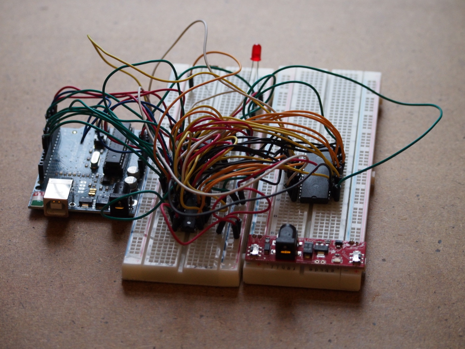
The breadboard circuit with the Arduino and ICs
The result is somewhat overwhelming! Presented in a more transparent fashion, and with some jumper wires replaced with breadboard wires, it is slightly easier to follow:
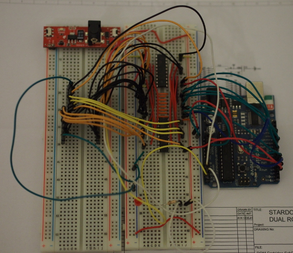
An overview of the breadboard circuit
The orange wires between the two chips on the right-hand breadboard indicate how the 8 Arduino pins are connected beyond the two flip-flop chips and directly to the flash memory chip, which would sit on the left-hand breadboard between the headers inserted into that breadboard (which weren’t used in the previous arrangement).
Making a Circuit Board
It should be pretty clear that while breadboarding can help a lot with prototyping, things can get messy very quickly with even moderately complicated circuits. And while I was prototyping this, I was running out of jumper wires that I needed for other things! Although this circuit is useful, I don’t want to have to commit my collection of components to keeping it available “just in case”, but at the same time I don’t want to have to wire it up when I do need it. The solution to this dilemma was obvious: I should make a “proper” printed circuit board (PCB) and free up all my jumper wires!
It is easy to be quickly overwhelmed when thinking about making circuit boards. Various people recommend various different tools for designing them, ranging from proprietary software that might be free-of-charge in certain forms but which imposes arbitrary limitations on designs (as well as curtailing your software freedoms) through to Free Software that people struggle to recommend because they have experienced stability or functionality deficiencies with it. And beyond the activity of designing boards, the act of getting them made is confused by the range of services in various different places with differing levels of service and quality, not to mention those people who advocate making boards at home using chemicals that are, shall we say, not always kind to the skin.
Fortunately, I had heard of an initiative called Fritzing some time ago, initially in connection with various interesting products being sold in an online store, but whose store then appeared to be offering a service – Fritzing Fab – to fabricate individual circuit boards. What isn’t clear, or wasn’t really clear to me straight away, was that Fritzing is also some Free Software that can be used to design circuit boards. Conveniently, it is also available as a Debian package.
The Fritzing software aims to make certain tasks easy that would perhaps otherwise require a degree of familiarity with the practice of making circuit boards. For instance, having decided that I wanted to interface my circuit to an Arduino as a shield which sits on top and connects directly to the connectors on the Arduino board, I can choose an Arduino shield PCB template in the Fritzing software and be sure that if I then choose to get the board made, the dimensions and placement of the various connections will all be correct. So for my purposes and with my level of experience, Fritzing seems like a reasonable choice for a first board design.
Replicating the Circuit
Fritzing probably gets a certain degree of disdain from experienced practitioners of electronic design because it seems to emphasise the breadboard paradigm, rather than insisting that a proper circuit diagram (or schematic) acts as the starting point. Here is what my circuit looks like in Fritzing:
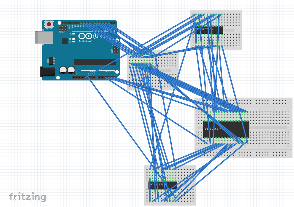
The breadboard view of my circuit in Fritzing
You will undoubtedly observe that it isn’t much tidier than my real-life breadboard layout! Having dragged a component like the Arduino Uno (mostly compatible with the Duemilanove) onto the canvas along with various breadboards, and then having dragged various other components onto those breadboards, all that remains is that we wire them up like we managed to do in reality. Here, Fritzing helps out by highlighting connections between things, so that breadboard columns appear green as wires are connected to them, indicating that an electrical connection is made and applies to all points in that column on that half of the breadboard (the upper or lower half as seen in the above image). It even highlights things that are connected together according to the properties of the device, so that any attempt to modify to a connection that leads to one of the ground pins on the Arduino also highlights the other ground pins as the modification is being done.
I can certainly understand criticism of this visual paradigm. Before wiring up the real-life circuit, I typically write down which things will be connected to each other in a simple table like this:
| Arduino | 74HC273 #1 | 74HC273 #2 | Am29F010 |
|---|---|---|---|
| A5 | CE# | ||
| A4 | OE# | ||
| A3 | WE# | ||
| 2 | CP | ||
| 3 | CP | ||
| 4 | D3 | D3 | DQ3 |
If I were not concerned with prototyping with breadboards, I would aim to use such information directly and not try and figure out which size breadboard I might need (or how many!) and how to arrange the wires so that signals get where they need to be. When one runs out of points in a breadboard column and has to introduce “staging” breadboards (as shown above by the breadboard hosting only incoming and outgoing wires), it distracts from the essential simplicity of a circuit.
Anyway, once the circuit is defined, and here it really does help that upon clicking on a terminal/pin, the connected terminals or pins are highlighted, we can move on to the schematic view and try and produce something that makes a degree of sense. Here is what that should look like in Fritzing:
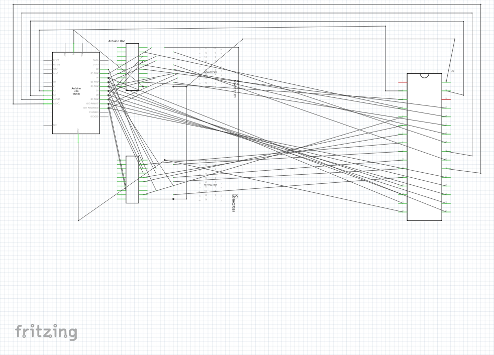
The schematic for the circuit in Fritzing
Now, the observant amongst you will notice that this doesn’t look very tidy at all. First of all, there are wires going directly between terminals without any respect for tidiness whatsoever. The more observant will notice that some of the wires end in the middle of nowhere, although on closer inspection they appear to be aimed at a pin of an IC but are shifted to the right on the diagram. I don’t know what causes this phenomenon, but it would seem that as far as the software is concerned, they are connected to the component. (I will come back to how components are defined and the pitfalls involved later on.)
Anyway, one might be tempted to skip over this view and try and start designing a PCB layout directly, but I found that it helped to try and tidy this up a bit. First of all, the effects of the breadboard paradigm tend to manifest themselves with connections that do not really reflect the logical relationships between components, so that an Arduino pin that feeds an input pin on both flip-flop ICs as well as a data pin on the flash memory IC may have its connectors represented by a wire first going from the Arduino to one of the flip-flop ICs, then to the other flip-flop IC, and finally to the flash memory IC in some kind of sequential wiring. Although electrically this is not incorrect, with a thought to the later track routing on a PCB, it may not be the best representation to help us think about such subsequent problems.
So, for my own sanity, I rearranged the connections to “fan out” from the Arduino as much as possible. This was at times a frustrating exercise, as those of you with experience with drawing applications might recognise: trying to persuade the software that you really did select a particular thing and not something else, and so on. Again, selecting the end of a connection causes some highlighting to occur, and the desired result is that selecting a terminal highlights the appropriate terminals on the various components and not the unrelated ones.
Sometimes that highlighting behaviour provides surprising and counter-intuitive results. Checking the breadboard layout tends to be useful because Fritzing occasionally thinks that a new connection between certain pins has been established, and it helpfully creates a “rats nest” connection on the breadboard layout without apparently saying anything. Such “rats nest” connections are logical connections that have not been “made real” by the use of a wire, and they feature heavily in the PCB view.
PCB Layout
For those of us with no experience of PCB layout who just admire the PCBs in everybody else’s products, the task of laying out the tracks so that they make electrical sense is a daunting one. Fritzing will provide a canvas containing a board and the chosen components, but it is up to you to combine them in a sensible way. Here, the circuit board actually corresponds to the Arduino in the breadboard and schematic views.
But slightly confusing as the depiction of the Arduino is in the breadboard view, the pertinent aspects of it are merely the connectors on that device, not the functionality of the device itself which we obviously aren’t intending to replicate. So, instead of the details of an actual Arduino or its functional equivalent, we instead merely see the connection points required by the Arduino. And by choosing a board template for an Arduino shield, those connection points should appear in the appropriate places, as well as the board itself having the appropriate size and shape to be an Arduino shield.
Here’s how the completed board looks:
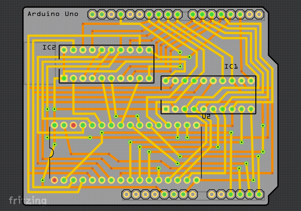
The upper surface of the PCB design in Fritzing
Of course, I have spared you a lot of work by just showing the image above. In practice, the components whose outlines and connectors feature above need to be positioned in sensible places. Then, tracks need to be defined connecting the different connection points, with dotted “rats nest” lines directly joining logically-connected points needing to be replaced with physical wiring in the form of those tracks. And of course, tracks do not enjoy the same luxury as the wires in the other views, of being able to cross over each other indiscriminately: they must be explicitly routed to the other side of the board, either using the existing connectors or by employing vias.

The lower surface of the PCB design in Fritzing
Hopefully, you will get to the point where there are no more dotted lines and where, upon selecting a connection point, all the appropriate points light up, just as we saw when probing the details of the other layouts. To reassure myself that I probably had connected everything up correctly, I went through my table and inspected the pin-outs of the components and did a kind of virtual electrical test, just to make sure that I wasn’t completely fooling myself.
With all this done, there isn’t much more to do before building up enough courage to actually get a board made, but one important step that remains is to run the “design checks” via the menu to see if there is anything that would prevent the board from working correctly or from otherwise being made. It can be the case that tracks do cross – the maze of yellow and orange can be distracting – or that they are too close and might cause signals to go astray. Fortunately, the hours of planning paid off here and only minor adjustments needed to be done.
It should be noted that the exercise of routing the tracks is certainly not to be underestimated when there are as many connections as there are above. Although an auto-routing function is provided, it failed to suggest tracks for most of the required connections and produced some bizarre routing as well. But clinging onto the memory of a working circuit in real three-dimensional space, along with the hope that two sides of a circuit board are enough and that there is enough space on the board, can keep the dream of a working design alive!
The Components
I skipped over the matter of components earlier on, and I don’t really want to dwell on the matter too much now, either. But one challenge that surprised me given the selection of fancy components that can be dragged onto the canvas was the lack of a simple template for a 32-pin DIP (dual in-line package) socket for the Am29F010 chip. There were socket definitions of different sizes, but it wasn’t possible to adjust the number of pins.
Now, there is a parts editor in Fritzing, but I tend to run away from graphical interfaces where I suspect that the matter could be resolved in more efficient ways, and it seems like other people feel the same way. Alongside the logical definition of the component’s connectors, one also has to consider the physical characteristics such as where the connectors are and what special markings will be reproduced on the PCB’s silk-screen for the component.
After copying an existing component, ransacking the Fritzing settings files, editing various files including those telling Fritzing about my new parts, I achieved my modest goals. But I would regard this as perhaps the weakest part of the software. I didn’t resort to doing things the behind-the-scenes way immediately, but the copy-and-edit paradigm was incredibly frustrating and doesn’t seem to be readily documented in a way I could usefully follow. There is a Sparkfun tutorial which describes things at length, but one cannot help feeling that a lot of this should be easier, especially for very simple component changes like the one I needed.
The Result
With some confidence and only modest expectations of success, I elected to place an order with the Fritzing Fab service and to see what the result would end up like. This was straightforward for the most part: upload the file created by Fritzing, fill out some details (albeit not via a secure connection), and then proceed to payment. Unfortunately, the easy payment method involves PayPal, and unfortunately PayPal wants random people like myself to create an account with them before they will consider letting me make a credit card payment, which is something that didn’t happen before. Fortunately, the Fritzing people are most accommodating and do support wire transfers as an alternative payment method, and they were very responsive to my queries, so I managed to get an order submitted even more quickly than I thought might happen (considering that fabrication happens only once a week).
Just over a week after placing my order, the board was shipped from Germany, arriving a couple of days later here in Norway. Here is what it looked like:
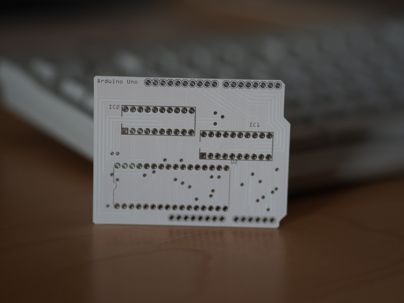
The finished PCB from Fritzing
Now, all I had to do was to populate the board and to test the circuit again with the Arduino. First, I tested the connections using the Arduino’s 5V and GND pins with an LED in series with a resistor in an “old school” approach to the problem, and everything seemed to be as I had defined it in the Fritzing software.
Given that I don’t really like soldering things, the act of populating the board went about as well as expected, even though I could still clean up the residue from the solder a bit (which would lead me onto a story about buying the recommended chemicals that I won’t bother you with). Here is the result of that activity:
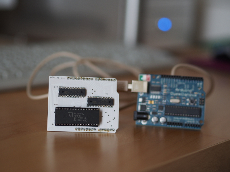
The populated board together with the Arduino
And, all that remained was the task of getting my software running and testing the circuit in its new form. Originally, I was only using 16 address pins, holding the seventeenth low, and had to change the software to handle these extended addresses. In addition, the issuing of commands to the flash memory device probably needed a bit of refinement as well. Consequently, this testing went on for a bit longer than I would have wished, but eventually I managed to successfully replicate the programming of a ROM image that had been done some time ago with the breadboard circuit.
The outcome did rely on a certain degree of good fortune: the template for the Arduino Uno is not quite compatible with the Duemilanove, but this was rectified by clipping two superfluous pins from one of the headers I soldered onto the board; two of the connections belonging to the socket holding the flash memory chip touch the outside of the plastic “power jack” socket, but not enough to cause a real problem. But I would like to think that a lot of preparation dealt with problems that otherwise might have occurred.
Apart from liberating my breadboards and wires, this exercise has provided useful experience with PCB design. And of course, you can find the sources for all of this in my repository, as well as a project page for the board on the Fritzing projects site. I hope that this account of my experiences will encourage others to consider trying it out, too. It isn’t as scary as it would first appear, after all, although I won’t deny that it was quite a bit of work!