Shared-Mode Executables in L4Re for MIPS-Based Devices
Sunday, July 8th, 2018I have been meaning to write about my device driver experiments with L4Re, following on from my porting exercises, but that exercise took me along various routes and I haven’t yet got back to documenting all of them. Meanwhile, one thing that did start to bother me was how much space the software was taking up when compiled, linked and ready to deploy.
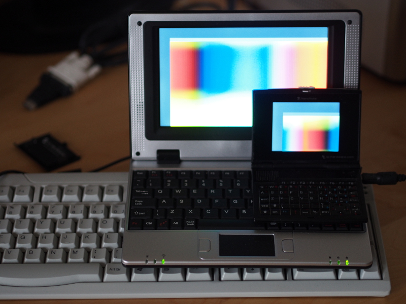
Since each of my device drivers is a separate program, and since each one may be linked to various libraries, they each started to contribute substantially to the size of the resulting file – the payload – needing to be transferred to the device. At one point, I had to resize the boot partition on the memory card used by the Letux 400 notebook computer to make the payload fit in the available space.
The work done to port L4Re to the MIPS Creator CI20 had already laid the foundations for functioning payloads, and once the final touches were put in place to support the peculiarities of the Ingenic JZ4780 system-on-a-chip, it was possible to run both the conventional “hello” example which is statically linked to its libraries, as well as a “shared-hello” example which is dynamically linked to its libraries. The latter configuration of the program results in a smaller executable program and thus a smaller payload.
So it seemed clear that I might be able to run my own programs on the Letux 400 or Ben NanoNote with similar reductions in payload size. Unfortunately, nothing ever seems to be as straightforward as it ought to be.
Exceptional Obstructions and Observations
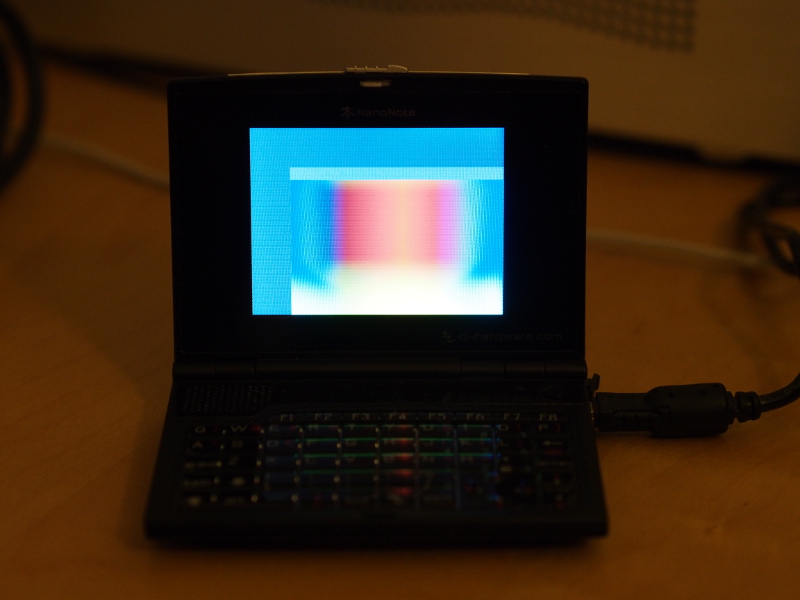
Initially, I set about trying one of my own graphical examples with the MODE variable set to “shared” in its Makefile. This, upon powering up, merely indicated that it had not managed to start up properly. Instead of a blank screen, the viewports set up by the graphical multiplexer, Mag, were still active and showing their usual blankness. But these regions did not then change in any way when I pressed keys on the keyboard (which is functionality that I will hopefully get round to describing in another article).
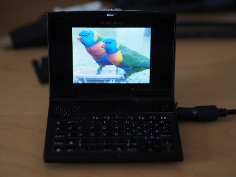
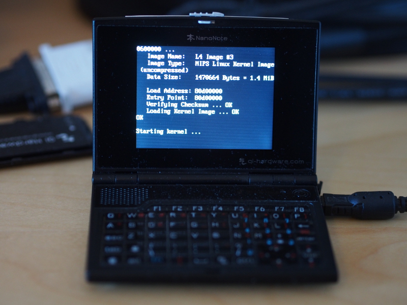
I sought some general advice from the l4-hackers mailing list, but quickly realised that to make any real progress, I would need a decent way of accessing the debugging output produced by the dynamic linker. This took me on a diversion that led to my debugging capabilities being strengthened with the availability of a textual output console on the screen of my devices. I still don’t like the idea of performing hardware modifications to get access to the serial console, so this is a useful and welcome alternative.
Having switched out the “hello” program with the “shared-hello” program in the system configuration and module list demonstrating the framebuffer terminal, I deployed the payload and powered up, but I did not get the satisfying output of the program operating normally. Instead, the framebuffer terminal appeared and rewarded me with the following message:
L4Re: rom/ex_hello_shared: Unhandled exception: PC=0x800000 PFA=8d7a LdrFlgs=0
This isn’t really the kind of thing you want to see. Having not had to debug L4Re or Fiasco.OC in any serious fashion for a couple of months, I was out of practice in considering the next step, but fortunately some encouragement arrived in a private e-mail from Jean Wolter. This brought the suggestion of triggering the kernel debugger, but since this requires serial console access, it wasn’t a viable approach. But another idea that I could use involved writing out a bit more information in the routine that was producing this output.
The message in question originates in the pkg/l4re-core/l4re_kernel/server/src/region.cc file, within the Region_map::op_exception method. The details it produces are rather minimal and generic: the program counter (PC) tells us where the exception occurred; the loader flags (LdrFlags) presumably tell us about the activity of the library loader; the mysterious “PFA” is supposedly the page fault address but it actually seemed to be the stack pointer address on these MIPS-based systems.
On their own, these details are not particularly informative, but I suppose that more useful information could quickly become fairly specific to a particular architecture. Jean suggested looking at the structure describing the exception state, l4_exc_regs_t (defined with MIPS-specific members in pkg/l4re-core/l4sys/include/ARCH-mips/utcb.h), to see what else I might dig up. This I did, generating the following:
pc=0x800000
gp=0x82dd30
sp=0x8d7a
ra=0x802f6c
cause=0x1000002c
A few things interested me, thus motivating my choice of registers to dump. The global pointer (gp) register tells us about symbols in the problematic code, and I felt that having once made changes to the L4Re sources – way back in the era of getting the CI20 to run GCC-generated code – so that another register (t9) would be initialised correctly, this so that the gp register would be set up correctly within programs, it was entirely possible that I had rather too enthusiastically changed something that was now causing a problem.
The stack pointer (sp) is useful to check, just to see if it located in a sensible region of memory, and here I discovered that this seemed to be the same as the “PFA” number. Oddly, the “PFA” seems to occupy the same place in the exception structure as any “bad virtual address” featuring in an address exception, and so I started to suspect that maybe the stack pointer was referencing the wrong part of memory. But this was partially ruled out by examining the value of the stack pointer in the “hello” example, which appeared to reference broadly the same part of memory. And, of course, the “hello” example works just fine.
In fact, the cause register indicated another kind of exception entirely, and it was one I was not really expecting: a “coprocessor unusable” exception indicating that coprocessor 1, typically a floating point arithmetic unit, was being illegally requested by an instruction. Here is how I interpreted that register’s value:
hex value   binary value
1000002c == 00010000000000000000000000101100
              --                     -----
              CE                     ExcCode

=> CE == 1; ExcCode == 11 (coprocessor unusable)
=> coprocessor 1 unusable
Now, as I may have mentioned before, the hardware involved in this exercise does not support floating point instructions itself, and this is why I have configured compilers to use “soft-float” (software-based floating point arithmetic) support. It meant that I had to find places that might have wanted to use floating point instructions and eliminate those instructions somehow. Fortunately, only code generated by the compiler was likely to contain such instructions. But now I wondered if there weren’t some instructions of this nature lurking in places I hadn’t checked.
I had also thought to check the return address (ra) register. This tells us where the processor will jump to when it has finished executing the current routine, and since this is usually a matter of “returning” somewhere, it tells us something about the code that was being executed before the problematic routine was called. I figured that the work being done before the exception was probably going to be more important than the exception itself.
Floating Point Magic
Another debugging suggestion that now became unavoidable was to inspect the erroneous instruction. I noted above that this instruction was causing the processor to signal an illegal attempt to use an unusable – actually completely unavailable – coprocessor. Writing a numeric representation of the instruction to the display provided me with the following hexadecimal (base 16) value:
464c457f
This can be interpreted as follows in binary, with groups of bits defined for interpretation according to the MIPS instruction set architecture, and with tentative interpretations of these groups provided beneath:
010001 10010  01100 01000 10101 111111
COP1   rs/fmt rt/ft rd/fs       C.ABS.NGT
The first group of bits is the opcode field which is interpreted as a coprocessor 1 (COP1) opcode. Should we then wish to consider what the other groups mean, we might then examine the final group which could indicate a comparison instruction. However, this becomes rather hypothetical since the processor will most likely interpret the opcode field and then decide that it cannot handle the instruction.
So, I started to look for places where the instruction might have been written, but no obvious locations were forthcoming. One peculiar aspect of all this is that the location of the instruction is at a rather “clean” location – 0x800000 – and some investigations indicated that this is where the library containing the problematic code gets loaded. I actually don’t remember precisely how I figured this out, but I think it was as follows.
I had looked at linker scripts that might give some details of the location of program objects, and one of them (pkg/l4re-core/ldscripts/ARCH-mips/main_dyn.ld) seemed to be related. It gave an address for the code of 0x400000. This made me think that some misconfiguration or erroneous operation was putting the observed code somewhere it shouldn’t be. But changing this address in the linker script just gave another exception at 0x400000, meaning that I had disrupted something that was intentional and probably working fine.
Meanwhile, emitting the t9 register’s value from the exception state yielded 0x800000, indicating that the calling routine had most likely jumped straight to that address, not to another address with execution having then proceeded normally until reaching the exception location. I decided to look at the instructions around the return address, these most likely being the ones that had set up the call to the exception location. Writing these locations out gave me some idea about the instructions involved. Below, I provide the stored values and their interpretations as machine instructions:
8f998250 # lw $t9, -32176($gp)
24a55fa8 # addiu $a1, $a1, 0x5fa8
0320f809 # jalr $t9
24844ee4 # addiu $a0, $a0, 0x4ee4
8fbc0010 # lw $gp, 16($sp)
One objective of doing this, apart from confirming that a jump instruction (jalr) was involved, with the t9 register being employed as is the convention with MIPS code, was to use the fragment to identify the library that was causing the error. A brute-force approach was employed here, generating “object dumps” from the library files and writing them out as files in a new directory:
mkdir tmpdir
for FILENAME in mybuild/lib/mips_32/l4f/* ; do
    mipsel-linux-gnu-objdump -d "$FILENAME" > tmpdir/`basename "$FILENAME"`
done
The textual dump files were then searched for the instruction values using grep, narrowing down the places where these instructions were found in consecutive locations. This yielded the following code, found in the libld-l4.so library:
    2f5c:       8f998250        lw      t9,-32176(gp)
    2f60:       24a55fa8        addiu   a1,a1,24488
    2f64:       0320f809        jalr    t9
    2f68:       24844ee4        addiu   a0,a0,20196
    2f6c:       8fbc0010        lw      gp,16(sp)
The integer operands for the addiu instructions are the same, of course, just being shown as decimal rather than hexadecimal values. Now, we previously saw that the return address (ra) register had the value 0x802f6c. When a MIPS processor executes a jump instruction, it will also fetch the following instruction and execute it, this being a consequence of the way the processor architecture is designed.
So, the instruction after the jump, residing in what is known as the “branch delay slot” is not the instruction that will be visited upon returning from the called routine. Instead, it is the instruction after that. Here, we see that the return address from the jump at location 0x2f64 would be two locations later at 0x2f6c. This provides a kind of realisation that the program object – the libld-l4.so library – is positioned in memory at 0x800000: 0x2f6c added to 0x800000 gives the value of ra, 0x802f6c.
And this means that the location of the problematic instruction – the cause of our exception – is the first location within this object. Anyone with any experience of this kind of software will have realised by now that this doesn’t sound like a healthy situation: the first location within a library is not actually going to be code because these kinds of objects are packaged up in a way that permits their manipulation by other programs.
So what is the first location of a library used for? Since such objects employ the Executable and Linkable Format (ELF), we can take a look at some documentation. And we see that the first location is used to identify the kind of object, employing a “magic number” for the purpose. And that magic number would be…
464c457f
In the little-endian arrangement employed by this processor, the stored bytes are as follows:
7f
45 ('E')
4c ('L')
46 ('F')
The value was not a floating point instruction at all, but the magic number at the start of the library object! It was something of a coincidence that such a value would be interpreted as a floating point instruction, an accidentally convenient way of signalling something going badly wrong.
Missing Entries
The investigation now started to focus on how the code trying to jump to the start of the library had managed to get this incorrect address and what it was trying to do by jumping to it. I started to wonder if the global pointer (gp), whose job it is to reference the list of locations of program routines and other global data, might have been miscalculated such that attempts to load the addresses of routines would then be failing with data being fetched from the wrong places.
But looking around at code fragments where the gp register was being calculated, they seemed to look set to calculate the correct values based on assumptions about other registers. For example, from the object dump for libld-l4.so:
00002780 <_ftext>:
    2780:       3c1c0003        lui     gp,0x3
    2784:       279cb5b0        addiu   gp,gp,-19024
    2788:       0399e021        addu    gp,gp,t9
Assuming that the processor has t9 set to 0x2780 and then jumps to the value of t9, as is the convention, the following calculation is then performed:
gp = 0x30000 (since lui loads the "upper" half-word)
gp = gp - 19024 = 0x30000 - 19024 = 0x2b5b0
gp = gp + t9 = 0x2b5b0 + 0x2780 = 0x2dd30
Using the nm tool, which tells us about symbols in program objects, it was possible to check this value:
mipsel-linux-gnu-nm -n mybuild/lib/mips_32/l4f/libld-l4.so
This shows the following at the end of the output:
0002dd30 d _gp
Also appearing somewhat earlier in the output is this, telling us where the table of symbols starts (as well as the next thing in the file):
00025d40 a _GLOBAL_OFFSET_TABLE_
00025f90 g __dso_handle
Some digging around in the L4Re source code gave a kind of confirmation that the difference between _gp and _GLOBAL_OFFSET_TABLE_ was to be expected. Here is what I found in the pkg/l4re-core/uclibc/lib/contrib/uclibc/ldso/ldso/mips/elfinterp.c file:
#define OFFSET_GP_GOT 0x7ff0
If gp, when recalculated in other places, ended up getting the same value, there didn’t seem to be anything wrong with it. Some quick inspections of neighbouring calculations indicated that this wasn’t likely to be the problem. But what about the values used in conjunction with gp? Might they be having an effect? In the case of the erroneous jump, the following calculation is involved:
lw t9,-32176(gp) => load word into t9 from the location at gp - 32176
                 => ...               from 0x2dd30 - 32176
                 => ...               from 0x25f80
The calculated address, 0x25f80, is after the start of _GLOBAL_OFFSET_TABLE_ providing entries for program routines and other things, which is a good sign, but what is perhaps more troubling is how far after the start of the table such a value is. In the above output, another symbol (__dso_handle) indicates something that is located at the end of the table. Now, although its address is still greater than the one computed above, meaning that the computation does not cause us to stray off the end of the table, the computed address is suspiciously close to the end.
There was nothing else to do than to have a look at the table contents itself, and here it was rather useful to have a way of displaying a number of values on the screen. At this point, we have to note that the addresses in use in the running system are adjusted according to the start of the loaded object, so that the table is positioned at 0x25d40 in the object dump, but in the running system we would see 0x800000 + 0x25d40 and thus 0x825d40 instead.
What I saw was that the table contained entries that varied in the expected way right up until 0x825f60 (corresponding to 0x25f60 in the object dump) being only 0x30 (or 48 bytes, or 12 entries) before the end of the table, but then all remaining entries starting at 0x825f64 (corresponding to 0x25f64) yielded a value of 0x800000, apart from 0x825f90 (corresponding to 0x25f90, right at the end of the table) which yielded itself.
Since the calculated address above (0x25f80, adjusted to 0x825f80 in the running system) lies in this final region, we now know the origin of this annoying 0x800000: it comes from entries at the end of the table that do not seem to hold meaningful values. Indeed, the object dump for the library seemed to skip over this region of the table entirely, presumably because it was left uninitialised. And using the readelf tool with the –relocs option to show “relocations”, which applies to this table, it appeared that the last entries rather confirmed my observations:
00025d34  00000003 R_MIPS_REL32
00025f90  00000003 R_MIPS_REL32
Clearly, something is missing from this table. But since something has to adjust the contents of the table to add the “base address”, 0x800000, to the entries in order to provide valid addresses within the running program, what started to intrigue me was whether the code that performed this adjustment had any idea about these missing entries, and how this code might be related to the code causing the exception situation.
Routines and Responsibilities
While considering the nature of the code causing the exception, I had been using the objdump utility with the -d (disassemble) and -D (disassemble all) options. These provide details of program sections, code routines and the machine instructions themselves. But Jean pointed out that if I really wanted to find out which part of the source code was responsible for producing certain regions of the program, I might use a combination of options: -d, -l (line numbers) and -S (source code). This was almost a revelation!
However, the code responsible for the jump to the start of the library resisted such measures. A large region of code appeared to have no corresponding source, suggesting that it might be generated. Here is how it starts:
_ftext():
    2dac:       00000000        nop
    2db0:       3c1c0003        lui     gp,0x3
    2db4:       279caf80        addiu   gp,gp,-20608
    2db8:       0399e021        addu    gp,gp,t9
    2dbc:       8f84801c        lw      a0,-32740(gp)
    2dc0:       8f828018        lw      v0,-32744(gp)
There is no function defined in the source code with the name _ftext. However, _ftext is defined in the linker script (in pkg/l4re-core/ldscripts/ARCH-mips/main_rel.ld) as follows:
  .text           :
  {
    _ftext = . ;
    *(.text.unlikely .text.*_unlikely .text.unlikely.*)
    *(.text.exit .text.exit.*)
    *(.text.startup .text.startup.*)
    *(.text.hot .text.hot.*)
    *(.text .stub .text.* .gnu.linkonce.t.*)
    /* .gnu.warning sections are handled specially by elf32.em.  */
    *(.gnu.warning)
    *(.mips16.fn.*) *(.mips16.call.*)
  }
If you haven’t encountered linker scripts before, then you probably don’t want to spend too much time looking at this, linker scripts being frustratingly terse and arcane, but the essence of the above is that a bunch of code is stuffed into the .text section, with _ftext being assigned the address of the start of all this code. Now, _ftext in the linker script corresponds to a particular label in the object dump (which we saw earlier was positioned at 0x2780) whereas the _ftext function in the code occurs later (at 0x2dac, above). After the label but before the function is code whose source is found by objdump.
So I took the approach of removing things from the linker script, ultimately removing everything from the .text section apart from the assignment to _ftext. This removed the annotated regions of the code and left me with only the _ftext function. It really did appear that this was something the compiler might be responsible for. But where would I find the code responsible?
One hint that was present in the _ftext function code was the use of another identified function, __cxa_finalize. Searching the GCC sources for code that might use it led me to the libgcc sources and to code that invokes destructor functions upon program exit. This wasn’t really what I was looking for, but the file containing it (libgcc/crtstuff.c) would prove informative.
Back to the Table
Jean had indicated that there might be a difference in output between compilers, and that certain symbols might be produced by some but not by others. I investigated further by using the readelf tool with the -a option to show almost everything about the library file. Here, the focus was on the global offset table (GOT) and information about the entries. In particular, I wanted to know more about the entry providing the erroneous 0x800000 value, located at (gp – 32176). In my output I saw the following interesting thing:
 Global entries:
   Address     Access  Initial Sym.Val. Type    Ndx Name
  00025f80 -32176(gp) 00000000 00000000 FUNC    UND __register_frame_info
This seems to tell us what the program expects to find at the location in question, and it indicates that the named symbol is presumably undefined. There were some other undefined symbols, too:
_ITM_deregisterTMCloneTable
_ITM_registerTMCloneTable
__deregister_frame_info
Meanwhile, Jean was seeing symbols with other names:
__register_frame_info_base
__deregister_frame_info_base
During my perusal of the libgcc sources, I had noticed some of these symbols being tested to see if they were non-zero. For example:
  if (__register_frame_info)
    __register_frame_info (__EH_FRAME_BEGIN__, &object);
These fragments of code appear to be located in functions related to program initialisation. And it is also interesting to note that back in the library code, after the offending table entry has been accessed, there are tests against zero:
    2f34:       3c1c0003        lui     gp,0x3
    2f38:       279cadfc        addiu   gp,gp,-20996
    2f3c:       0399e021        addu    gp,gp,t9
    2f40:       27bdffe0        addiu   sp,sp,-32
    2f44:       8f828250        lw      v0,-32176(gp)
    2f48:       afbc0010        sw      gp,16(sp)
    2f4c:       afbf001c        sw      ra,28(sp)
    2f50:       10400007        beqz    v0,2f70 <_ftext+0x7f0>
Here, gp gets set up correctly, v0 is set to the value of the table entry, which we now believe refers to __register_frame_info, and the beqz instruction tests this value against zero, skipping ahead if it is zero. Does that not sound a bit like the code shown above? One might think that the libgcc code might handle an uninitialised table entry, and maybe it is intended to do so, but the table entry ends up getting adjusted to 0x800000, presumably as part of the library loading process.
I think that the most relevant function here for the adjustment of these entries is _dl_perform_mips_global_got_relocations which can be found in the pkg/l4re-core/uclibc/lib/contrib/uclibc/ldso/ldso/ldso.c file as part of the L4Re C library code. It may well have changed the entry from zero to this erroneous non-zero value, merely because the entry lies within the table and is assumed to be valid.
So, as a consequence, the libgcc code acts as if it has a genuine __register_frame_info function to call, and doing so causes the jump to the start of the library object and the exception. Maybe the code is supposed to be designed to handle missing symbols, those symbols potentially being deliberately omitted, but it doesn’t function correctly under these particular circumstances.
Symbol Restoration
However, despite identifying this unfortunate interaction between C library and libgcc, the matter of a remedy remained unaddressed. What was I to do about these missing symbols? Were they supposed to be there? Was there a way to tell libgcc not to expect them to be there at all?
In attempting to learn a bit more about the linking process, I had probably been through the different L4Re packages several times, but Jean then pointed me to a file I had seen before, perhaps before I had needed to think about these symbols at all. It contained “empty” definitions for some of the symbols but not for others. Maybe the workaround or even the solution was to just add more definitions corresponding to the symbols the program was expecting? Jean thought so.
So, I added a few things to the file (pkg/l4re-core/ldso/ldso/fixup.c):
void __deregister_frame_info(void);
void __register_frame_info(void);
void _ITM_deregisterTMCloneTable(void);
void _ITM_registerTMCloneTable(void);

void __deregister_frame_info(void) {}
void __register_frame_info(void) {}
void _ITM_deregisterTMCloneTable(void) {}
void _ITM_registerTMCloneTable(void) {}
I wasn’t confident that this would fix the problem. After all the investigation, adding a few lines of trivial code to one file seemed like too easy a way to fix what seemed like a serious problem. But I checked the object dump of the library, and suddenly things looked a bit more reasonable. Instead of referencing an uninitialised table entry, objdump was able to identify the jump target as __register_frame_info:
    2e14:       8f828040        lw      v0,-32704(gp)
    2e18:       afbc0010        sw      gp,16(sp)
    2e1c:       afbf001c        sw      ra,28(sp)
    2e20:       10400007        beqz    v0,2e40 <_ftext+0x7f0>
    2e24:       8f85801c        lw      a1,-32740(gp)
    2e28:       8f84803c        lw      a0,-32708(gp)
    2e2c:       8f998040        lw      t9,-32704(gp)
    2e30:       24a55fa8        addiu   a1,a1,24488
    2e34:       04111c39        bal     9f1c <__register_frame_info>
Of course, the code had been reorganised and so things were no longer in quite the same places, but in the above, (gp – 32704) is actually a reference to __register_frame_info, and although this value gets tested against zero as before, we can see that enough is now known about the previously-missing symbol that a branch directly to the location of the function has been incorporated, rather than a jump to the address stored in the table.
And sure enough, powering up the Letux 400 produced the framebuffer terminal showing the expected output:
Hi World! (shared)
It had been a long journey for such a modest reward, but thanks to Jean’s help and a bit of perseverance, I got there in the end.